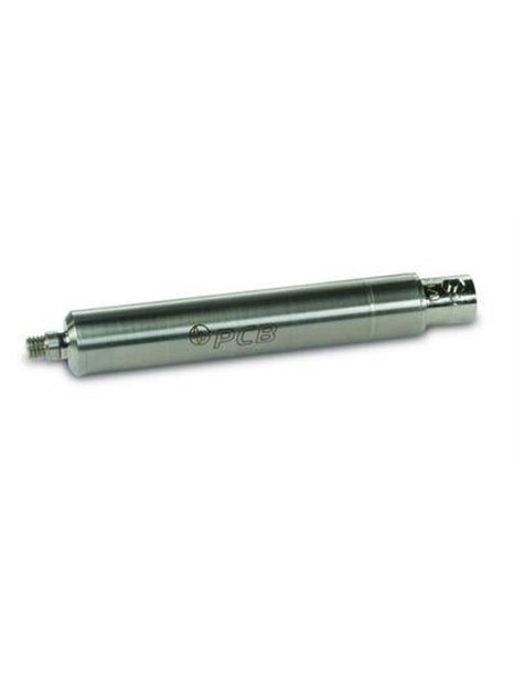
PCB-422E54
- Inline charge amplifier,
- Input range ±50. 000 pC,
- Output range ±5 V,
- Transcription factor: 0.1 mV / pC,
- Frequency range 5 … 50,000 Hz (depends on the constant current)
| basic data | |||
| Transfer factor (± 2.5%) | 0.1 mV / pC | ||
| entrance area | ± 50,000 pC | ||
| Overload range | ± 8 V | ||
| Lower limit frequency (-5%) | 5 Hz | ||
| Upper limit frequency (constant current 4 mA) | 12,000 Hz | [2] | |
| Upper limit frequency (constant current 20 mA) | 50,000 Hz | [2] | |
| linearity error | 1.0% FS | ||
| Operating conditions | |||
| The temperature range (operation) | -65 ... 250 ° F | -54 ... 121 ° C | |
| Maximum shock resistance | 5000 g pk | 49,050 m / s pk | |
| Maximum acceleration (5) | 100 g pk | 981 m / spk | |
| Technical characteristics | |||
| supply voltage | 18 ... 28 V DC | ||
| Constant current supply | 2 ... 20 mA | ||
| output range | ± 5.0 V | ||
| output impedance | 100 ? | ||
| Bias voltage | 9 ... 13 V DC | ||
| Maximum voltage at the sensor input | 40 V | ||
| Broadband noise (1 ... 10,000 Hz) | 33 uV | -90 dB | [1] |
| Spectral Noise (1 Hz) | 9.8 µV/ ?Hz | -100 dB | [1] |
| Spectral noise (10 Hz) | 3 µV/ ?Hz | -110 dB | [1] |
| Spectral noise (100 Hz) | 0.8 uV / Hz | -122 dB | [1] |
| Spectral noise (1,000 Hz) | 0.4 µV/ ?Hz | -128 dB | [1] |
| Spectral noise (10,000 Hz) | 0.2 µV/ ?Hz | -134 dB | [1] |
| Capacitance (feedback branch of the amplifier) | 10,000 pF | ||
| Recovery time after overdriving | 10 microseconds | ||
| discharging | > 0.1 s | ||
| Resistance (the feedback branch of the amplifier) | 60 MΩ | [3] | |
| Influence of input capacitance (sensor + cable) to transfer factor | 0.0005% / pF | ||
| physical properties | |||
| housing material | stainless steel | ||
| seal | epoxy resin | ||
| Electrical connection (input) | 10-32 coaxial | ||
| Electrical connection (output) | BNC connector | ||
| Size - Diameter | 0.52 in | 13 mm | |
| Size - Length | 3.4 in | 86 mm | |
| Dimensions | 1.15 oz | 32.7 grams | |
| Hints | |||
| [1] | Tested with a voltage source and a capacitor (for the simulation of a sensor) | ||
| [2] | The upper frequency limit can be reduced by the amount of the constant current and the length of cable used on the output side. | ||
| [3] | Because of the upcoming used amplifier electronics the discharge time on the basis of three times the resistance value must be calculated in the feedback path. | ||
| [4] | Details: see PCB Declaration of Conformance PS024 . CE conformity is only guaranteed when the housing is grounded. |


