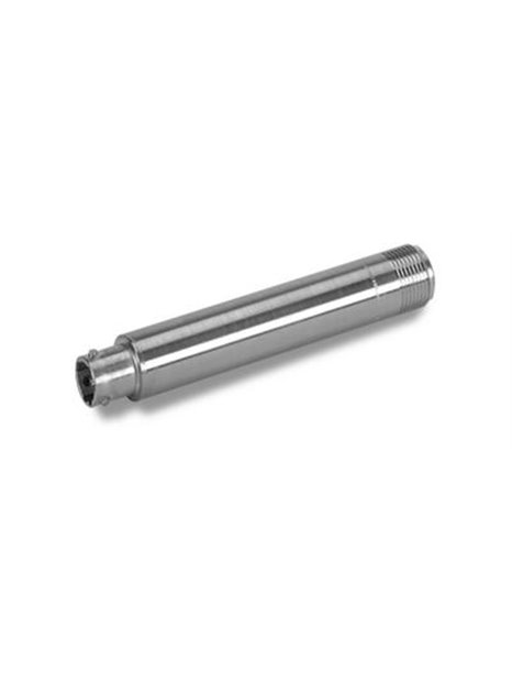
PCB-422E20
| basic data | |||
| transcription factor (±5%) | 4 mV / pC | ||
| Overload range | ±3 V | ||
| Lower limiting frequency (-5%) | 1 Hz | ||
| upper frequency limit (constant current 2.2 mA) | 50,000 Hz | [2] | |
| upper frequency limit ( Constant current 4 mA) | 75,000 Hz | [2] | |
| upper frequency limit (constant current 20 mA) | 100,000 Hz | [2] | |
| linearity error | ≤ 1.0% FS | ||
| conditions of use | |||
| temperature range (operation) | -65 … 250 ° F | -54 … 121 ° C | |
| influence of temperature on Transcription factor | < 1% | ||
| maximum shock resistance | 1,000 g pk | 9,810 m/s² PK | |
| Specifications | |||
| power supply | 18 … 28 V DC | ||
| Constant power supply | 2.2 … 20 mA | ||
| Output range | ±2. 5 V pk | ||
| output polarity | inverted | ||
| Output impedance | < 10 Ω | ||
| Bias voltage | 12.75 … 14.25 V DC | ||
| Maximum voltage at the sensor input | 30 V | ||
| Wide band noise (1 … 10,000 Hz) | 15 µV | -96 dB | [1] |
| spectral noise (1 Hz) | 10 µV / √ Hz | -100 dB | [1] |
| Spectral noise (10 Hz) | 0.8 µV / √ Hz | -122 dB | [1] |
| spectral noise (100 Hz) | 0.2 MV / √ Hz | -134 dB | [1] |
| Spectral noise (1,000 Hz) | 0.07 µV / √ Hz | 143 dB | [1] |
| spectral noise (10,000 Hz) | 0.07 µV / √ Hz | 143 dB | [1] |
| Discharging charging time constant | ≥ 0<5 s | ||
| minimal resistance at the sensor input | 5 M Ω | [3] | |
| influence of the input capacitance (sensor + cable) on transcription factor | 0.00≤5 %/pF | ||
| physical properties | |||
| go äusematerial | stainless steel | ||
| sealing | hermetically sealed welded | ||
| electrical connection (input) | 2-pin MIL-C-26482 | ||
| electrical connection (output) | 2-pin connector (MIL-C-5015) | ||
| size - diameter | 0.62 in | 16 mm | |
| Size - length | 3.62 in | 92.0 mm | |
| mass | 2.46 oz | 69.7 grams | |
| notes | |||
| [1] | tested with a voltage source and a capacitor (to simulate of a sensor) | ||
| [2] | above the specified rate, it comes to errors due to the low maximum rise and drop speed of the charge amplifier. | ||
| [3] | no use with low-impedance input resistances (especially not suitable for sensors, temperaturesare exposed to over?200 ? C) | ||
| [4] | details: see PCBs Declaration of conformance PS024. CE conformity is only guaranteed, if the housing is earthed. | ||
| (T) TEDS memory in accordance with IEEE PP1451. 4 | |||
| temperature range | -40 … 185 ° F | -40 … 85 ° C | |
| Bias voltage | 13.35 … 14.85 V DC |


